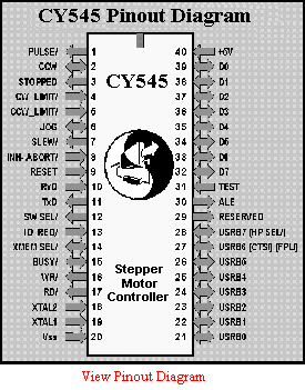
CY545 Dip Pinout & Dimensions
 .................................
 .......
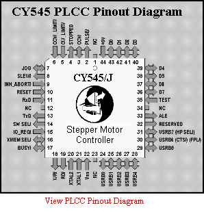
CY545/J PLCC Pinout & Dimensions
 .......................
 ......
......
CYCY545 DIP & CY545/J
PLCC Pin Descriptions
DIP PLCC Description
-    1      (O)   NC
1    2      (O)   PULSE/ Step pulse output, one pulse per step
2    3      (I/O) CCW Step direction
These pins run the stepper power driver. A high level on the direction
signal indicates counter clockwise direction, while a low level indicates
clockwise direction. The Pulse signal is normally high, going low at
the beginning of each step.
DIP PLCC Description
3 4 (O) STOPPED Motion status, low while stepping
This signal may be used to indicate motion complete, by its high level.
It may also control power selection for the stepper driver, switching
between high power for stepping, and parking power while stopped.
DIP PLCC Description
4    5     (I)    CW_LIMIT/ Clockwise step limit reached
5    6     (I)    CCW_LIMIT/ Counter Clockwise step limit reached
If either signal is low, it indicates a limit has been reached. The
CY545 will not continue stepping in that direction until the limit
signal is removed. Normal stepping is allowed in the opposite direc-
tion.
DIP PLCC Description
6 7 (I/O) JOG Manual stepping control
This signal is the manual stepping control input.  When it is floating,
the CY545 will not jog.  However, if the signal is connected to ground,
the CY545 will jog in the CW direction.  The jog step rate is derived
from the First Rate parameter and the normal Step Rate Table, by divid-
ing the selected rate by 20.  This gives a range of about 1 step per
second to about 1000 steps per second.  The input signal is always
enabled, and is tested by the CY545 while it is not executing another
command.
DIP PLCC Description
7    8     (I/O)  SLEW/ Slew indicator signal
8    9     (I)    INHIBIT_ABORT/ External motion control
This signal group indicates and controls motion status. SLEW/ indicates
when the maximum selected step rate has been achieved. If externally
driven low at the beginning of a motion, it also selects the continuous
step mode. INHIBIT_ABORT/ can hold off motion at the start or force an
early down ramp, then stop motion when the CY545 has ramped down to the
starting rate.
DIP PLCC Description
9    10    (I)    RESET CY545 hardware reset, active high pulse
10   11    (I)    RxD Received serial data into CY545
-    12    (O)    NC
11   13    (O)    TxD Transmitted serial data from CY545
These are TTL level serial data signals that can be used to issue com-
mands to or get replies from the CY545. Addition of an RS-232 voltage
level driver/receiver, such as the Maxim MAX233, allows any RS-232
device, such as the IBM PC COM1 port to talk directly to the CY545.
DIP PLCC Description
12 14 (O) SW_SEL/ Switch select
This signal is active when the CY545 is reading a parameter value from
external thumbwheel switches. The switch address is generated by the
parallel data bus.
DIP PLCC Description
13 15 (I) IO_REQUEST/ Parallel handshake input signal
This signal is driven low when a parallel command is issued to the
CY545. It is used as part of the parallel command handshake. If the
parallel command function is not used, this signal may select a fixed
serial baud rate as follows: 0 = 300 baud, 1 = 2400 baud, F = 9600 baud
DIP PLCC Description
14 16 (I/O) XMEM_SEL/ External local memory select
This signal goes low when the CY545 reads or writes to the local
external memory. Data and addresses are generated by the parallel data
bus. Up to 64K bytes of external memory are supported. When this signal
is driven low at power-up or reset, the CY545 will not test for the
Auto Start key sequence or automatically execute commands from the
external memory.
DIP PLCC Description
15 17 (I/O) BUSY/ Parallel handshake acknowledgement
BUSY/ is used with IO_REQUEST/ to implement the two line parallel com-
mand handshake. This signal indicates that the CY545 has accepted a
parallel data character from the device driving the IO_REQUEST signal.
If the parallel handshake is not used, this pin may be tied low to
select fixed baud rates through the IO_REQUEST signal.
DIP PLCC Description
16   18    (O)   WR/ Write strobe
17   19    (O)   RD/ Read strobe
These strobes are active while the CY545 is reading from the external
thumbwheel switches, display, or memory, or while it is writing to the
external display or memory.
DIP PLCC Description
18   20    (I)   XTAL2 Crystal connection
19   21    (I)   XTAL1 Crystal connection
An external crystal or clock source is connected to these pins, with a
value between 3.5 MHz and 16 MHz. For serial communications, an 11 MHz
crystal will give standard baud rates.
DIP PLCC Description
20   22    (I)   VSS Power supply ground.
-    23    (O)   NC
21   24    (I/O) USRB0 User selectable function, bit 0
22   25    (I/O) USRB1 User selectable function, bit 1
23   26    (I/O) USRB2 User selectable function, bit 2
24   27    (I/O) USRB3 User selectable function, bit 3
25   28    (I/O) USRB4 User selectable function, bit 4
26   29    (I/O) USRB5 User selectable function, bit 5
27   30    (I/O) USRB6 User selectable function, bit 6 or FPL/ or CTS/
28   31    (I/O) USRB7 User selectable function, bit 7 or HP_SEL/
This group of signals is used for multiple, user selectable functions,
including bit set and clear, bit test and branch, wait for signal value,
and auto home functions. Any function may be performed on any bit. Bits
6 and 7 also have fixed alternative functions of CY233 FPL control and
local parallel HP display selection if these features are used with the
CY545. If the application does not use a CY233, CTS/, or HP display,
these bits may be used for any other functions.
DIP PLCC Description
29   32    (O)   RESERVED Reserved signal, not used by CY545
30   33    (O)   ALE Address latch enable
The ALE signal is used to demultiplex the lower byte address from the data
bus during external memory, display, or thumbwheel switch operations.
-    34    (O)   NC
31   35    (I)   TEST Internal test signal, connect to Vcc.
DIP PLCC Description
32   36    (I/O) D7 Parallel data bus, bit 7, MSB
33   37    (I/O) D6 Parallel data bus, bit 6
34   38    (I/O) D5 Parallel data bus, bit 5
35   39    (I/O) D4 Parallel data bus, bit 4
36   40    (I/O) D3 Parallel data bus, bit 3
37   41    (I/O) D2 Parallel data bus, bit 2
38   42    (I/O) D1 Parallel data bus, bit 1
39   43    (I/O) D0 Parallel data bus, bit 0, LSB
This group is the parallel data bus, used to read or write parallel
data. During access to external thumbwheel switches, memory, or dis-
play, the lower byte of the device address is presented on these lines
just prior to the data transfer. Parallel commands are also accepted by
the CY545 on these lines, using the handshake control signals. These
lines are open drain, so external pull-up resistors are required when
they are used as outputs.
DIP PLCC Description
40 44 (I) VCC +5 Volt power supply input.
00 Contents ..|..
01 Intro ..|..
02 Pins & Packages ..|..
03 Cmd Interfaces ..|..
04 Commands..|..
05 Motor Cmds
06 Bit Cmds..|..
07 Memory Cmds..|..
08 Prog Branch Cmds..|..
09 Mode Cmds ..|..
10 Misc Cmds
11 Circuits ..|..
12 External Memory ..|..
13 Thumbwheel Switch
..|.. 14 Output
Display ..|..
15 Proto Boards
16 Timing & Control
..|.. 17 Rate
Tables ..|..
18 Electrical Specs ..|..
19 Examples ..|..
20 Up & Running
Back to CY545 Data Sheet
© 1988 - 1999 Cybernetic Micro Systems, Inc.
All rights reserved.
CY545 Manual 22MAR99